Ceramics Printed Circuit Boards
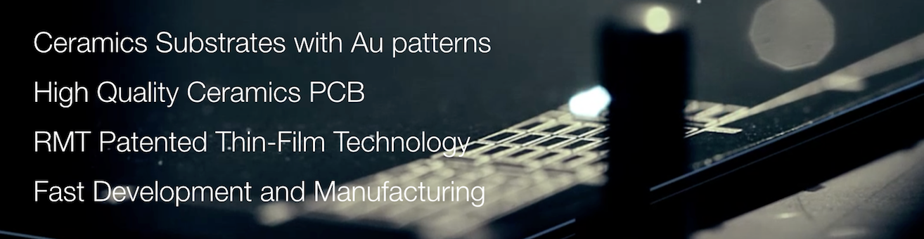
RMT Ltd provides full service with single and double-sided ceramics PCB and substrates manufacturing. The technology is developed and patented by RMT Ltd company. Company know-how allow to manufacture high quality ceramics substrates and PCB on Al2O3 and AlN materials. The key advantages are in precision patterns, high-quality processing, excellent solderability and bondability with single- and double-side metallized ceramics processing.
RMT patented technology provides significant advantages over typical thin- and thick-film metallization processes. Single and double-sided ceramics PCBs have better quality, higher resolution, high conductivity, excellent solderability and bonding properties.
RMT provide fast development and manufacturing of metallized ceramics substrates and ceramics PCBs for LD applications, optoelectronics industry, high-frequency and other applications.
 Fig.1 - RMT technology Metallization Structure (click to zoom) Fig.1 - RMT technology Metallization Structure (click to zoom) | 
Fig.2 - Ceramics PCB with VIAS (click to zoom) |
Ceramics Processing & Services
 |  |  | ||
| Various shape ceramics cutting | Various holes ceramics cutting | Double-side metallization process | ||
 |  |  | ||
| Precise customized Au patterns | Various ceramics thicknesses | Trial and volume manufacturing |
|
Parameter |
Ceramics Material |
Units |
Comments | ||
|
Al2O3(100%) |
Al2O3(96%) |
AlN(100%) | |||
|
General dimensions | |||||
|
Substrate footprint, max |
60.0 x 48.0 |
mm |
Default* | ||
|
Substrate thickness |
0.15; 0.25; 0.5; 0.63; 1.0 |
mm |
Default* | ||
|
Substrate surface |
|
|
| ||
|
- polished |
Ra < 0.1 |
um |
| ||
|
- lapped |
Ra < 0.4 |
um |
| ||
|
Pattern properties | |||||
|
Stripe width, min |
0.1 |
mm |
| ||
|
Between stripes, min |
0.1 (0.05*) |
mm |
| ||
|
Metallization adhesion |
> 5 |
> 3 |
> 3 |
kg/mm2 |
|
|
Double-sided metallization |
+ |
|
| ||
|
Via-holes diameter, minimum |
0.2 |
mm |
| ||
|
Alignment accuracy |
20 |
um |
For double-sided patterns | ||
|
Metallization | |||||
|
Adhesion layer, Cr (Ti) |
< 0.1 |
um |
Magnetron sputtering | ||
|
Conductive layer, Сu |
20 - 25 |
um |
Magnetron sputtering | ||
|
Barrier layer, Ni |
3 - 4 |
um |
Chemical deposition | ||
|
Finishing layer, Au |
0.2 - 0.3 |
um |
Chemical deposition | ||
|
Processing | |||||
|
Laser disc dicing |
+ |
|
| ||
|
Laser cutting/scribing |
+ |
|
| ||
|
VIAS |
+ |
|
Laser drilling | ||
|
* Parameters may be adjusted by request | |||||
RMT provide full service with Au patterned ceramics substrates (and ceramics PCB) development, prototyping and manufacturing. For additional info and requests, please, contact us directly.